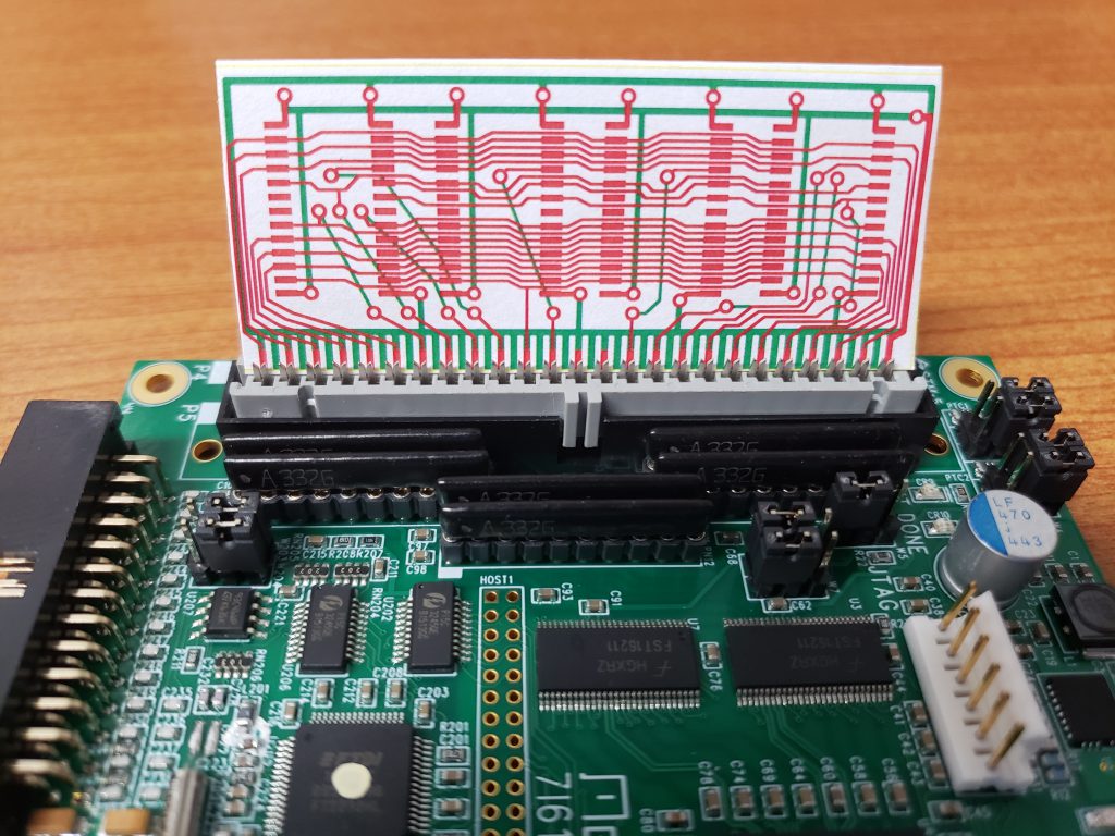
« Back to Blog   

Add Memory to a FPGA board
October 1, 2019
By Jeff K.

DRAM memory
DRAM memory board

For those projects requiring more memory, I have created a daughter board. This board may have up to 4 memory chips, each providing 16MBits of memory (2M x 4).

The MESA boards have 24 signals on each of their connectors. Finding memory requiring 24 or less signals was the trick. The 2M x 4 configuration has 19 signals: 11 address, 4 data, RAS, CAS, WE, and OE. I select one of the 4 memory chips by providing separate CAS.

About the Author
Jeff K.
Vintage Hardware Restoration Engineer
As a kid, Jeff became interested in how machines work after reading Benny the Bulldozer by Edith Thatcher Hurd (1947). In high school, Jeff took his first computing classes, including a math class that taught him to plot a spirograph on a HP 91000B calculator. Jeff eventually enjoyed a thirty-five year career as a technician with Strobe Data, before joining LCM+L’s engineering team to work on the Xerox Sigma 9 mainframe computer. Today you can find Jeff tinkering away upstairs on the IBM 360/30.

He continues to plot spirographs on computers.

Category Tags
Restoration